Friday, 27 February 2015
Task-7
Calculate the midgap voltage
The midgap voltage can be found by figuring
out the midgap capacitance first. By definition, the midgap capacitance is a
series capacitance with the oxide capacitance (which is the maximum capacitance)
and the depletion capacitance, namely,
where
From the lecture note, we obtain an
important information, which is that the under midgap condition,
therefore:
The interpretations of the required
variables are listed below:
Permittivity in free space - 8.85e(-12) F/M
Relative permittivity for silicon – 11.7
Charge carried by an electron – 1.602*10^(-19) C
Maximum capacitance (read from the given txt file) -2.92*10^3 pF
After calculation
Permittivity in free space - 8.85e(-12) F/M
Relative permittivity for silicon – 11.7
Charge carried by an electron – 1.602*10^(-19) C
Maximum capacitance (read from the given txt file) -2.92*10^3 pF
After calculation
From
the txt file, we can figure out the midgap voltage is between 1.36 and 1.37
volts.
Friday, 20 February 2015
Task-6
Calculate the flatband voltage.
The flatband condition is defined as the applied
voltage is 0, and in this case, the capacitance equals to the oxide capacitance
in series with the Debye capacitance. Which is:
From the reference handout
Where the Debye capacitance
The interpretation of the required
variables are listed below:
Permittivity in free space - 8.85e(-12) F/M
Relative permittivity for silicon – 11.7
Charge carried by an electron – 1.602e(-19)
Maximum capacitance (read from the given txt
file) - 2.919e3 pF
Acceptor concentration –
4.088e(21) /m^3
Capacitor area – 2.375829444e(-7)
Thermal voltage – 25 mV
Therefore,
The flatband capacitance is
According to the txt file, the flatband
voltage should be in the interval between 0.93 and 0.94 V.
Task-5
Calculate the work function difference assuming a gold (Au) gate.
Work function is defined as the energy
difference from the ‘fermi-level’ to the ‘vacuum level’.
For a metal,
work function is a
constant that can be measured.
For a semiconductor
, where
Xs is
electron affinity, and is 4.14eV for silicon.
Eg is
the band gap energy and is 1.1eV for silicon, Finally,
the last term is the Fermi level relative to the middle of the band gap, and can be calculated
using formula
.
Therefore
The function difference is
Task-4 Determine the doping density of the
silicon substrate
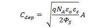
Doping density I associated with the work
function which is links the capacitance. One equation can be used to synthesise
the donor’s concentration.
The interpretation for the physical
quantities are listed underneath:
Capacitor area – 2.37589444e(-7)/m^2
Charge carried by an electron – 1.602e-(19) C
Boltzmann’s constant –
Room temperature – 300 K
Permittivity in free space - 8.85e(-12) F/m
Relative permittivity for silicon – 11.2
Silicon intrinsic carrier concentration –
10e15/m^3
Minimum capacitance (read from the given txt
file) – 53.4 pF
Maximum capacitance (read from the given txt
file) - 2.919e3 pF
Simplify the equation, we have
The result is a transcendental function of
, and MATLAB
was utilized to obtain the value of
. Two methods
were used.
- Method 1: Adopting the build-in function
The answer is clearly wrong because it
indicate there is no doping on the semiconductor.
- Method 2: Adopting the image method
Separate the equation with
the right hand side as
,
and left hand side as
After running the above program, a graph containing two curves
was displayed on screen.
The linear line represents
for the equation
and the curve represents for the right hand side equation
Clearly, the intersection is the desired value for
Because of the intersection is between 4e21 and 5e21, the domain of the doping concentration could be reduce to an interval between 3.5e21 and 5e21. The result is shown in figure 2.
In order to acquire a more
accurate value of doping concentration, ‘Data cursor’ under the tool bar was
utilized and the final approximation value is shown below:
Therefore, the doping concentration is approximately equal to 4.088e21/m^3
Wednesday, 11 February 2015
Task 3 The equivalent oxide thickness (EOT)
(12 February, 2015)
In recent years, some high-k materials are used in the MOSFET which take place of silicon dioxide. The equivalent oxide thickness is describe the thickness that the silicon dioxide need which to act as the same effect as the thickness of high-k material. There are two methods to solve the problem.
Method 1
using the equation
From the data we had, Cmax=2.92*10^-9 F
Solving the equation we have
EOT=2.808nm
Method 2
using the equaiton
simplify this equation, we get the equation about EOT
The end we get the EOT=2.8nm
Task 2 Determine the oxide relative permittivity
(12 February, 2015 )
The total capacitance is equal to the value of the oxide capacitance and the accumulation layer in series in accumulation stage.
so we have the equation


so we know that
and the oxide capacitance contains two parts which are high-k material and Silicon dioxide.
and we know that
the relationship of capacitance with permittivity
From the data, we get the maximum value of the capacitance is Cmax=2.92*10^-9 F. We know the diameter of capacitor is 0.55 mm, so the area of the capacitor is A=(d/2)^2*pi, and the thickness of high-k is t1=3.3nm and the thickness of silicon dioxide is t2=1.6nm.
Solving the equation [1][2][3][4][5][6]
we get the oxide relative permittivity k=10.65151148.
task 1 The type of substrate
( 11 February, 2015)
Firstly, we should learn some basic knowledge of MOSFET. We have received the data about the values of capacitance and voltage. We need to determine what type this substrate is from the C-V curve. therefore, we need to know the figures of n-type and p-type. In high-frequency, the figure 1 is the plot of n-type MOSFET [1] and figure 2 is the plot of p-type MOSFET [2].
figure 1
figure 2
Secondly, we used origin software to analysis the data and plot the curve of capacitance-voltage. The figure 3 shows the curve we got from the data,
Then, we could find this curve is similar with the curve of p-type. Therefore, this is a p-type substrate.
Reference list
[1] Kim, Hyoung-Sub,"HfO2-based InP n-channel metal-oxide-semiconductor field-effect transistors and metal-oxide-semiconductor capacitors using a germanium interfacial passivation layer" 2008, Vol. 93 Issue 10.
[2] Stauffer, Lee, "Fundamentals of Semiconductor C-V Measurements.” Evaluation Engineering,2008, Vol. 47 Issue 12, p20-24 。
Subscribe to:
Posts (Atom)